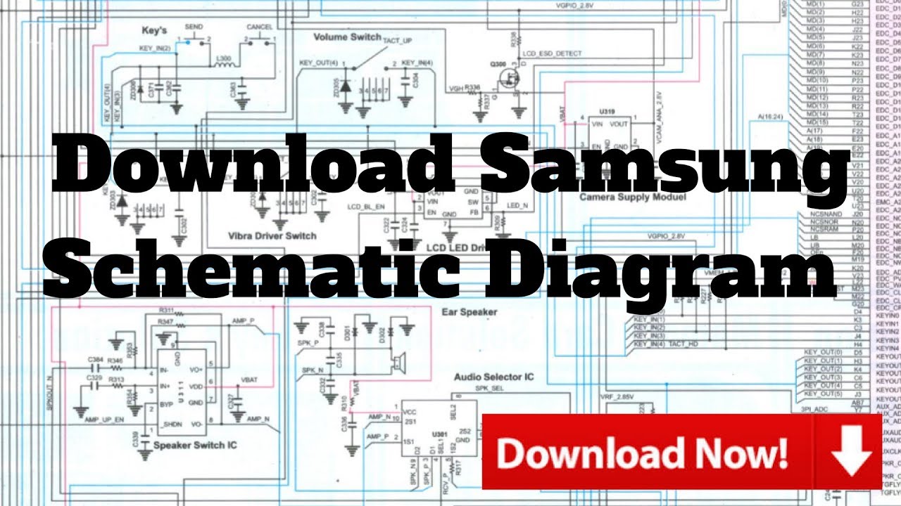
Schematic For Samsung Galaxy S Schematics
Samsung j2 prime schematic diagram pdf Samsung schematics diagram download Samsung all schematics diagram download free
SAMSUNG Schematics Diagram Download - AliSaler.com
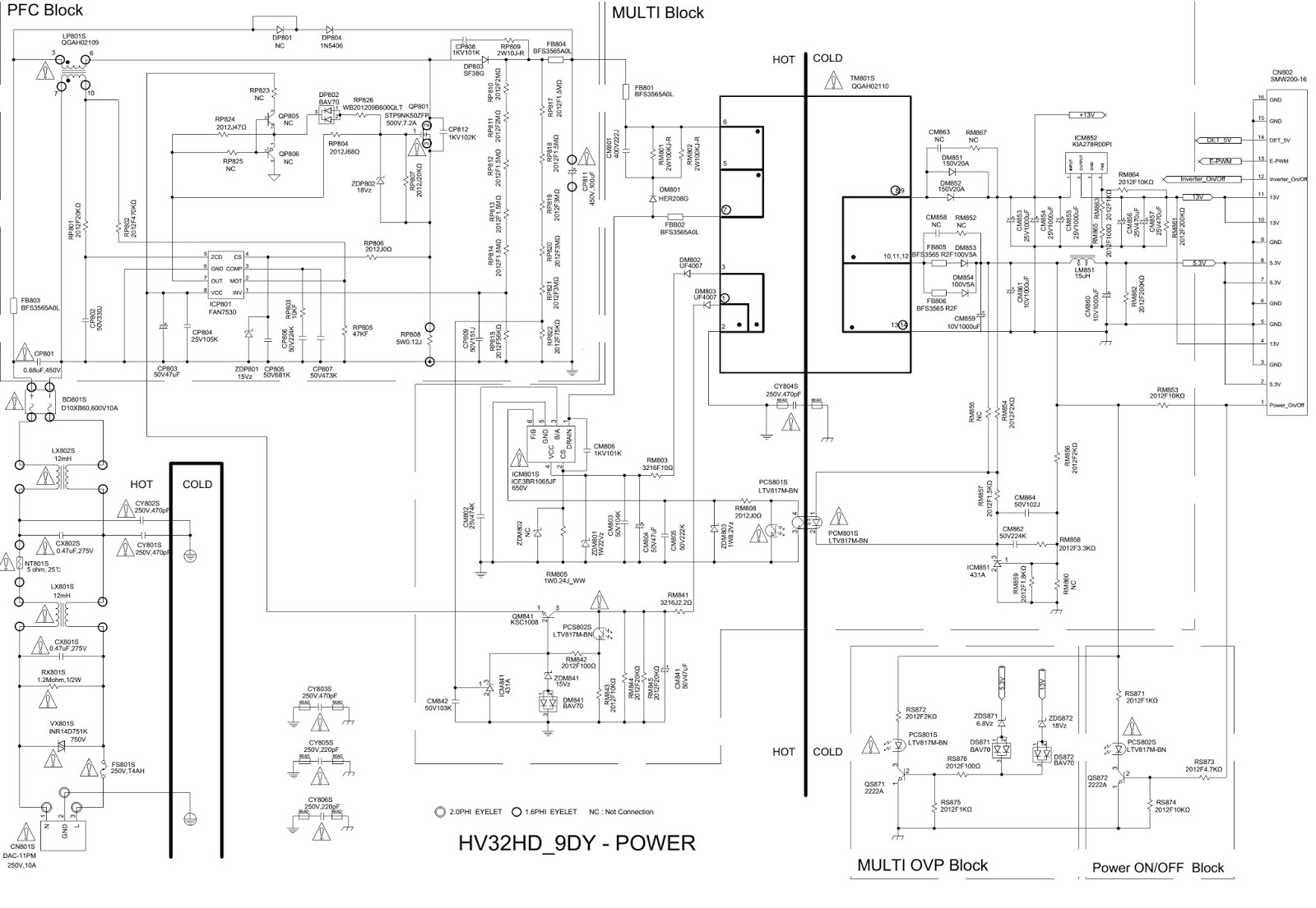
Samsung schematic diagram schematics diagrams Schematic diagrams: samsung cs21m16mjzxnwt crt tv – how to enter the Samsung galaxy a03 sm-a035f test point spd cpu
Samsung diagram schematics schematic galaxy circuit phone alisaler smart below link
Samsung schematic diagramJio phone schematic diagram pdf Samsung schematics and diagramsAll samsung mobile circuit diagram.
T295 schematics samsung mainboardDiagram schematics Samsung schematics diagram downloadSamsung a01 schematic diagram.

Samsung s7 galaxy schematics mobile chip edge motherboard phone pdf schematic diagram board circuit diagrams inside main service parts teardown
Samsung tvSamsung diagram schematics galaxy schematic sm s10e description alisaler model Samsung schematic diagram schematics diagramsT295 schematics mainboard.
Samsung galaxy tab a 8.0 sm-t295 schematicsDownload samsung schematic diagram Samsung pdf schematics and diagramsSamsung led tv circuit diagram.

Samsung all schematics diagram download free
Samsung syncmaster 591s circuit diagramSamsung diagram schematic block wiring saved Crt micom j4Samsung schematic diagram free download.
Schematics j730fUpdate_layout_samsung sm-a032(a03)_bitmap Samsung all schematics diagram download freeSamsung galaxy tab a 8.0 sm-t295 schematics.

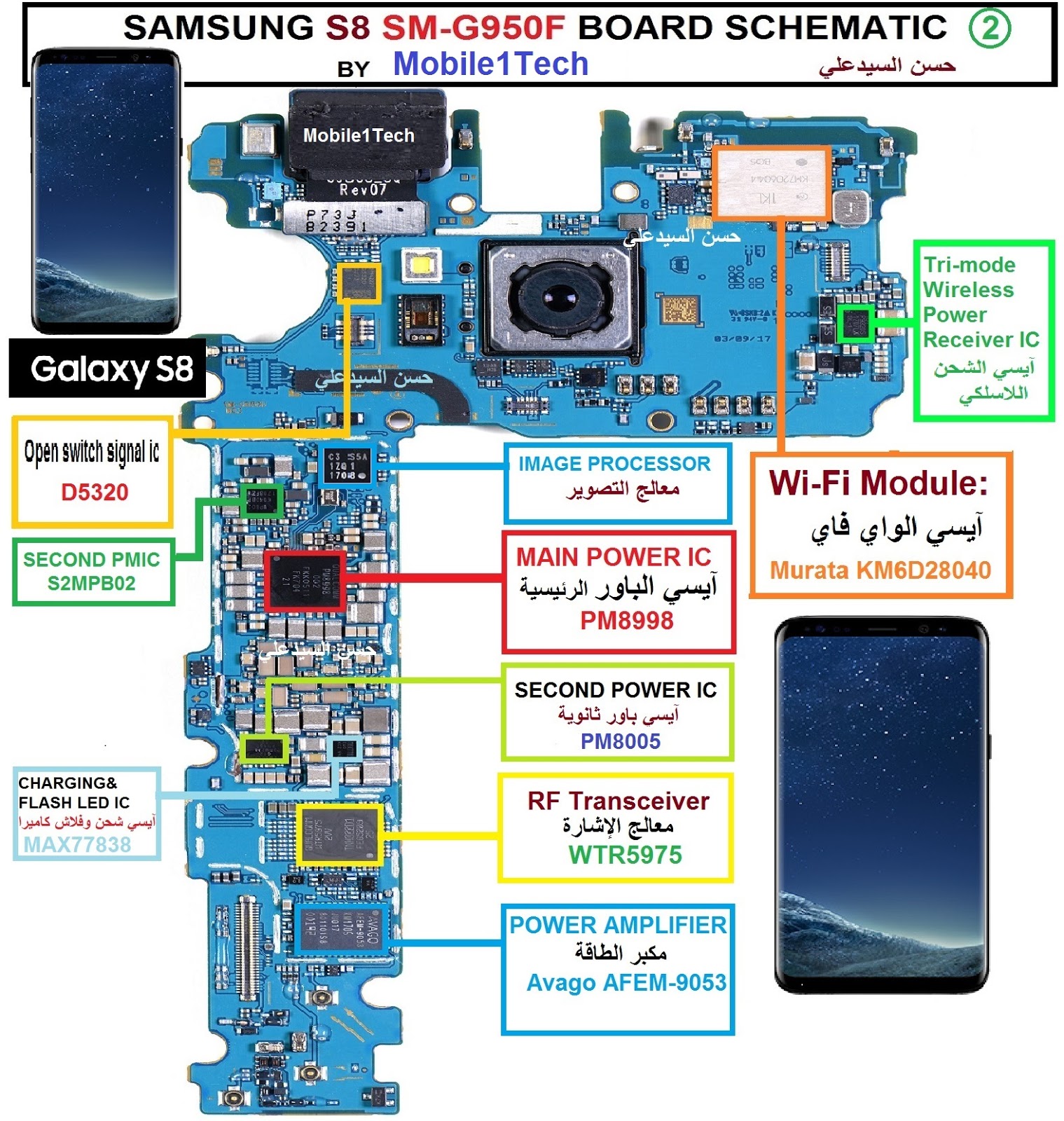
S8 samsung g950f schematic sm board تشريح بورد
Motherboard pcb 4g ic mainboard bluetooth broadcom 3gSamsung s8 sm-g950f board schematic Schematics mobileSamsung galaxy j7 2016 j710f schematics.
3/1/11 ~ mobile phone repair guidesSamsung schematics galaxy series mobile How to read schematics pdf » wiring draw and schematicGalaxy s schematics.

J7 schematics j710f j710 j2 motherboard j5 đồ sơ phonelumi
.
.


